Technical features

- The projection scanning lithography system is specifically designed to meet the patterning requirements of the copper grid line process for heterojunction cells. This system features rapid lithography, high resolution, and a large depth of focus. It uses a 405 nm fiber laser light source, and is very suitable for exposure on photovoltaic-specific photosensitive inks to form high-quality slot type structures.It is equipped with a CCD-based recognition system for substrate correction with an alignment precision of 30 μm.
- The projection scanning lithography mode adopts low-cost standard masks as graphic inputs, and has the advantages of good exposure uniformity and consistency, large process window, high adaptability to substrate thickness errors, and easy assembly with front-end and back-end equipment. It is an ideal solution for photovoltaic patterning.
Specifications

* The metrics may vary depending on the processes
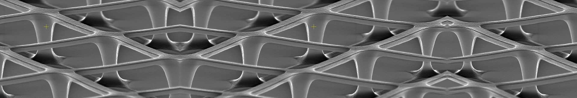
Lithography results using polished substrates with negative photoresists

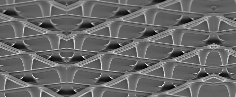
Lithography results using photovoltaic copper-plated substrates with photosensitive inks
